The board I am using only has a 4 digit seven segment display for output and 4 buttons for controlling the clock function as input
This project has multiple functions as shown below.
1.switching digit
2.disable or enable the alarm function
3.setting the clock digit (hour,minute,second)
4.setting the alarm clock digit (hour,minute,second)
5.counting down timer
Here is the illustration of function set
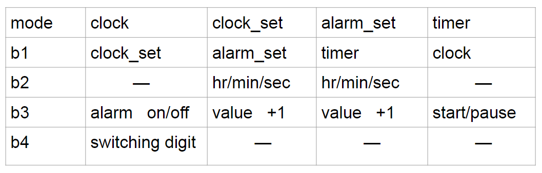
note: value +1 means the setting value would count up in cycle (ex:minute 00 ~ 59 ...)
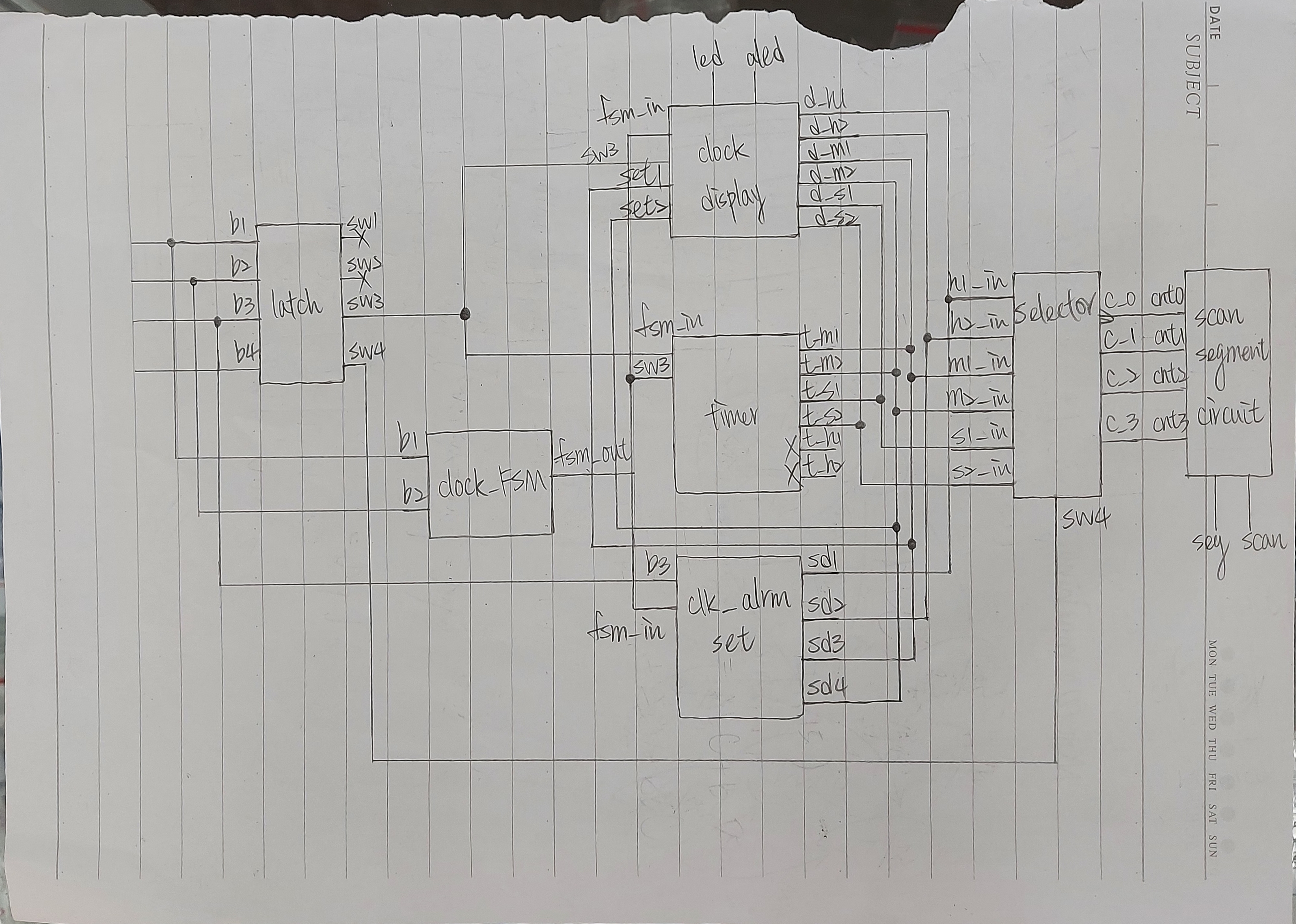
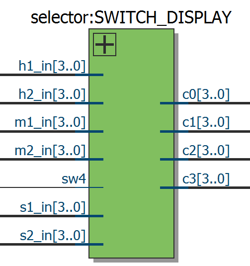
Before I built this project, I drew a sketch that described how many functional modules it needed and the connections between these functional modules. Considering the FPGA board I'm using, the board only has a 4-bit seven-segment and 5 buttons to use in this project. So I need to create a latch circuit to convert some buttons into switches, and create a selector to toggle the display numbers to display (hours:minutes:seconds).
Here you can see some of these functional modules and their connections. My idea is that I need other modules that correspond to the outputs of the finite state machine.
This is my main idea when I sketch.
And there is another RTL netlist diagram that is created by Quaturs after complited the entire VHDL coding.

The RTL netlist doesn't seem to be the same as the sketch, because I've added some external functions so that the whole hardware can function properly.
(ex: push button debounce,latch circuit for transiting the push button to mechanical switch...I would explain them later)

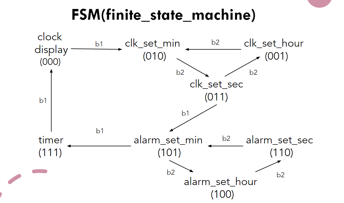
We replace the states shown on the state diagram with symbols (s0 ~ s7), and the decoding list can be found in the clock_FSM vhd file, i.e. coding comments.
b1 and b2 are the input of the Finite state machine, the binary number below the state is the output of Finite state machine.
Note that the clock feed in the FSM is only 2hz, the reason why the clock is incredibly slow is that if we increase the clock frequency, the state transitions are too fast to be viewed. So we need low frequencies to stabilize our FSM.
Here is a simple testbench result for simulating the FSM module.
 It can be seen from the simulation results that the defect of the Moore machine is that the current state transition is delayed by one cycle. But there is no delay in the output of the FSM, which guarantees that the entire function will not fail or crash.

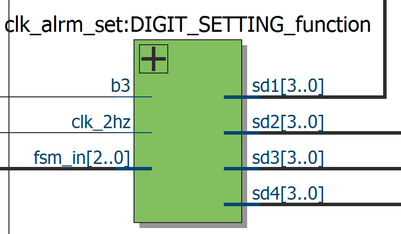
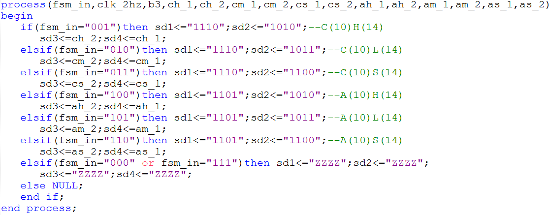
sd1,sd2: The sign of menu.
sd3:the first digit output.
sd4:the second digit output.
Tri-state is very important in this module to prevent data transfer at inappropriate time.

Here is a simple testbench result for simulating the clk_alrm_set module.
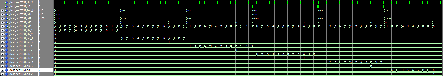
The purpose of the test is to check that the data outputs (sd3, sd4) are in sync with the registers and the results are in sync.
Take fsm_in as "001" as an example, now sd3 output should be synchronized with ch_1, sd4 should be synchronized with ch_2, sd1 and sd2 should output menu symbols
Here is a list of correspondences
fsm_in: "001" sd1 <-- "1110"(C) sd2 <-- "1010"(H)
sd3 <-- ch_1
sd4 <-- ch_2
fsm_in: "010" sd1 <-- "1110"(C) sd2 <-- "1011"(L)
sd3 <-- cm_1
sd4 <-- cm_2
fsm_in: "011" sd1 <-- "1110"(C) sd2 <-- "1100"(S)
sd3 <-- cs_1
sd4 <-- cs_2
fsm_in: "100" sd1 <-- "1101"(A) sd2 <-- "1010"(H)
sd3 <-- ah_1
sd4 <-- ah_2
fsm_in: "101" sd1 <-- "1101"(A) sd2 <-- "1011"(L)
sd3 <-- am_1
sd4 <-- am_2
fsm_in: "110" sd1 <-- "1101"(A) sd2 <-- "1100"(S)
sd3 <-- as_1
sd4 <-- as_2
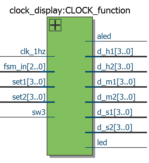
clk_1hz: clock input
sw3: toggle alarm mode on/off
fsm_in: signal of FSM
set1,set2: input data for refreshing digit
d_h1,d_h2,d_m1,d_m2,d_s1,d_s2: output the clock digit
led,aled: indicating the alarm mode
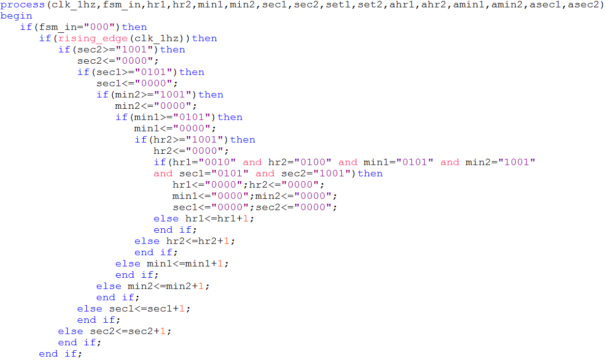
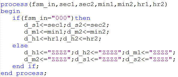
The clock function consists with two parts which are the display and receive/store data.These two parts correspond the input signal of FSM,you can check the list at the previous section.Here is the screenshot of part of the code.

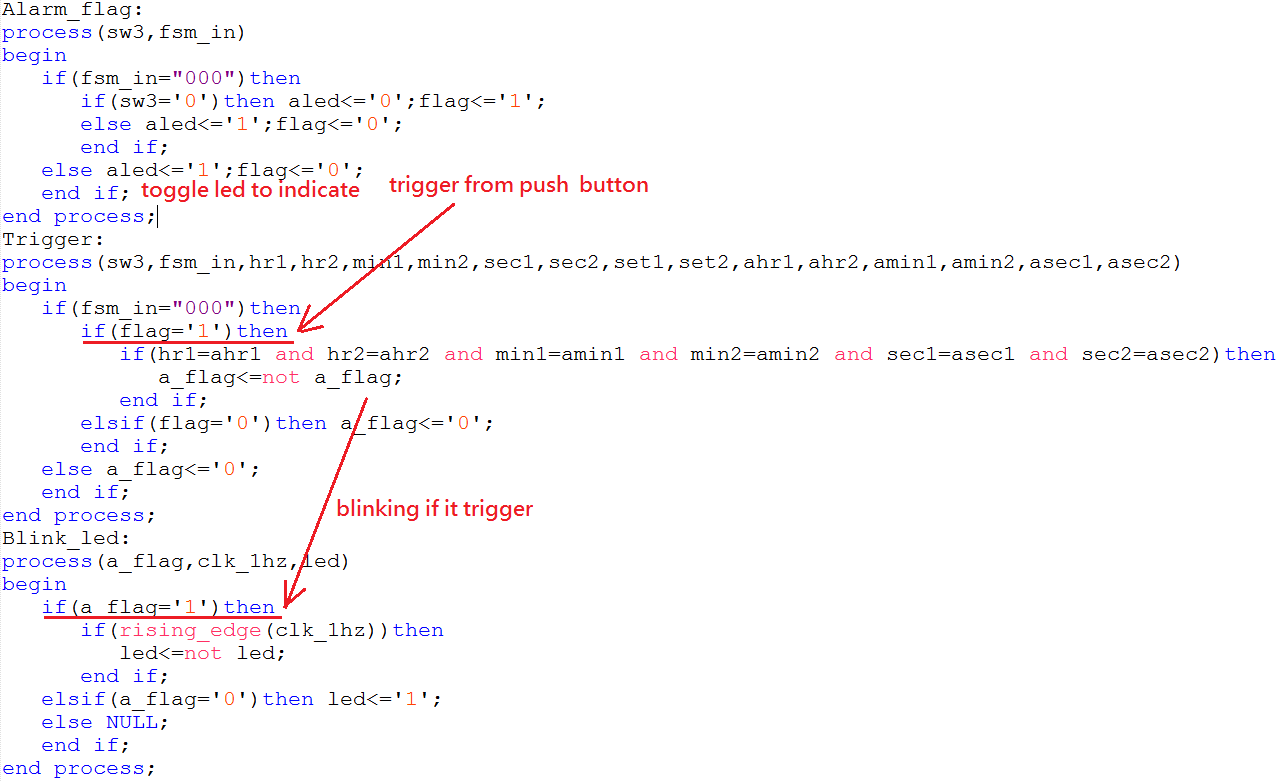
The alarm function has three parts which are "push button to trigger the alarm flag","check whether the clock digit match the alarm digit","if they match then blinking led".
Here is another screenshot describing the above statement.This module also has the tri-state to prevent,showing on the right hand side.
Here is a simple testbench for testing the clock function and alarm function and storing data.
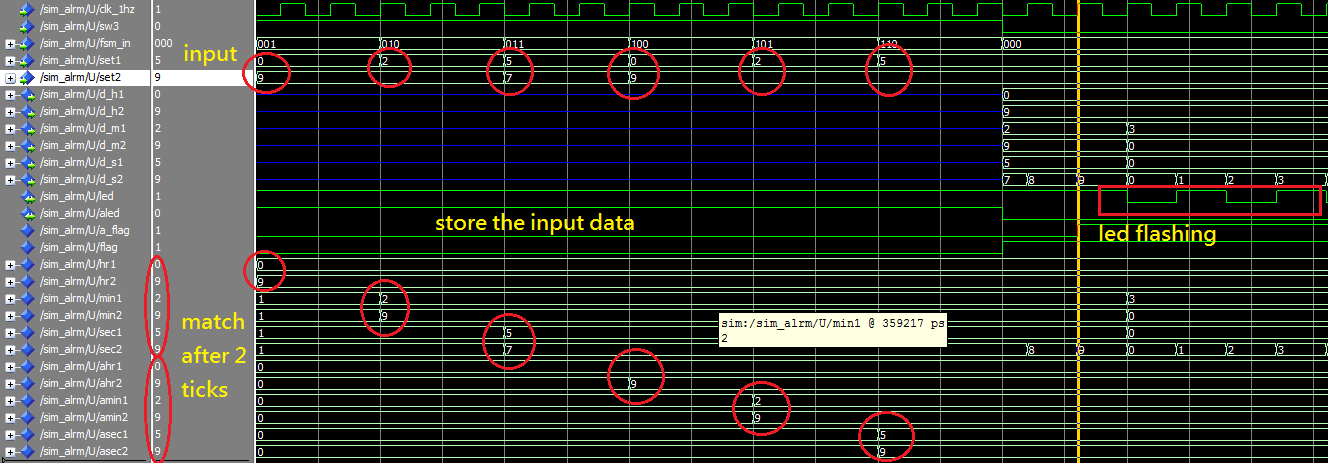
There exits one problem that I haven't fixed is that the data stored in the "Clock and alarm digit set" will force to refresh the digit of "clock display" while you press down the b1 to cycle the function menu.It will be fixed soon by adding more module.
The following modules are optional as they are custom made for the FPGA board I am using. After downloading the code, you can choose which module you want or remake them.


These modules are simple to understand and they are build for hardware aspect problem